
The QRSS-8P-1800 is ideally suited for battery-powered IoT nodes, smart utility networks, rail communications, healthcare wearables, and software-defined radio platforms requiring sub-6 GHz multi-standard coverage
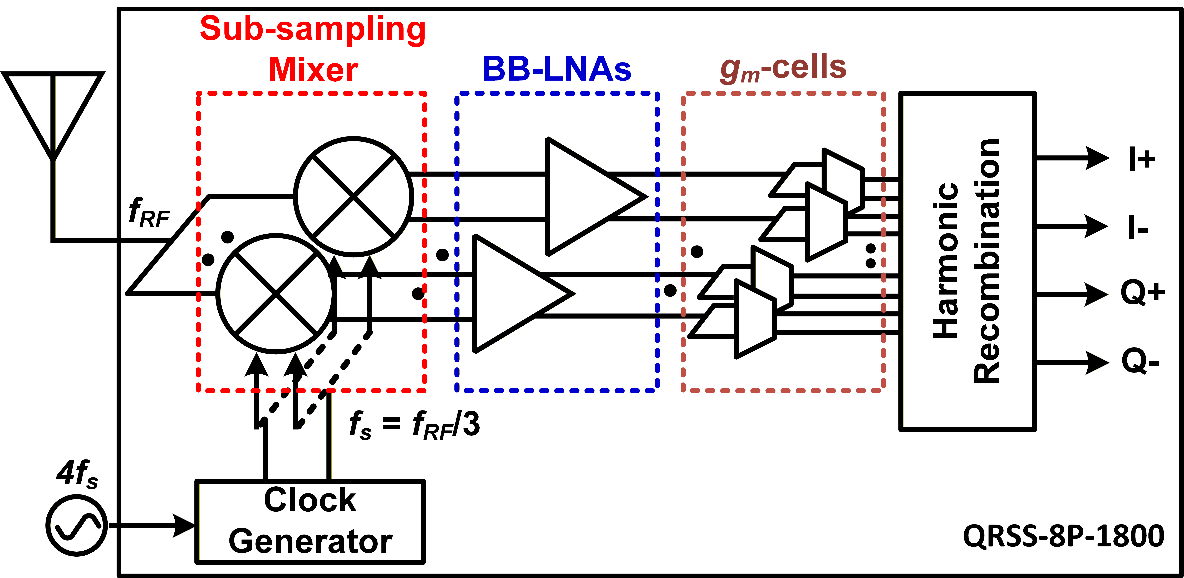
FAB & PROCESS SPECIFICATIONS
- Process Node: 65 nm CMOS (TSMC 1P9M)
- Active area:0.32 mm²
- Status: Silicon-Proven / Production-Ready
ARCHITECTURAL HIGHLIGHTS
- Direct (zero-IF) quadrature down-conversion
- Conversion Gain: 22 dB
- IB-IIP₃: −1 dBm | OB-IIP₃: +8 dBm
- 3-dB Bandwidth: 90 MHz
- Noise Figure: 4.7 dB
Power Consumption Power Consumption < 25 mW – Operating Temp Range -40°C to +85°C (Industrial)
The receiver is ideally suited for IEEE 802.11 WLAN systems, wireless access points, embedded Wi-Fi modules, software-defined radio (SDR) platforms, and other dual-band wireless communication applications.
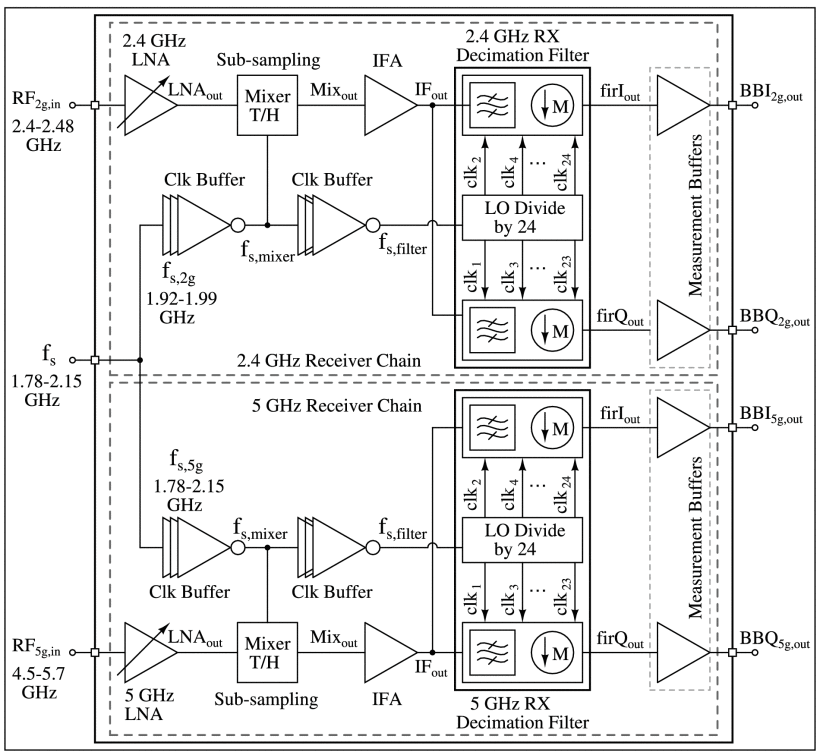
FAB & PROCESS SPECIFICATIONS
- Process Node: TSMC 65nm
- Active area:0.72mm
- Status: Silicon-Proven / Production-Ready
ARCHITECTURAL HIGHLIGHTS
- Direct RF-to-IF sub-sampling receiver architecture
- Continuously tunable gain: 26–41 dB (2.4 GHz), 26–38.5 dB (5 GHz)
- IIP₃: −8 dBm
- Signal bandwidth: 77 MHz
Power Consumption Power Consumption < 55 mW EVM -40 dB over 19 dB input power range Operating Temp Range -40°C to +125°C (Industrial)
The IP is ideally suited for low-power IoT devices, wireless sensor networks, smart metering, industrial automation, wearable electronics, and software-defined radio (SDR) platforms.
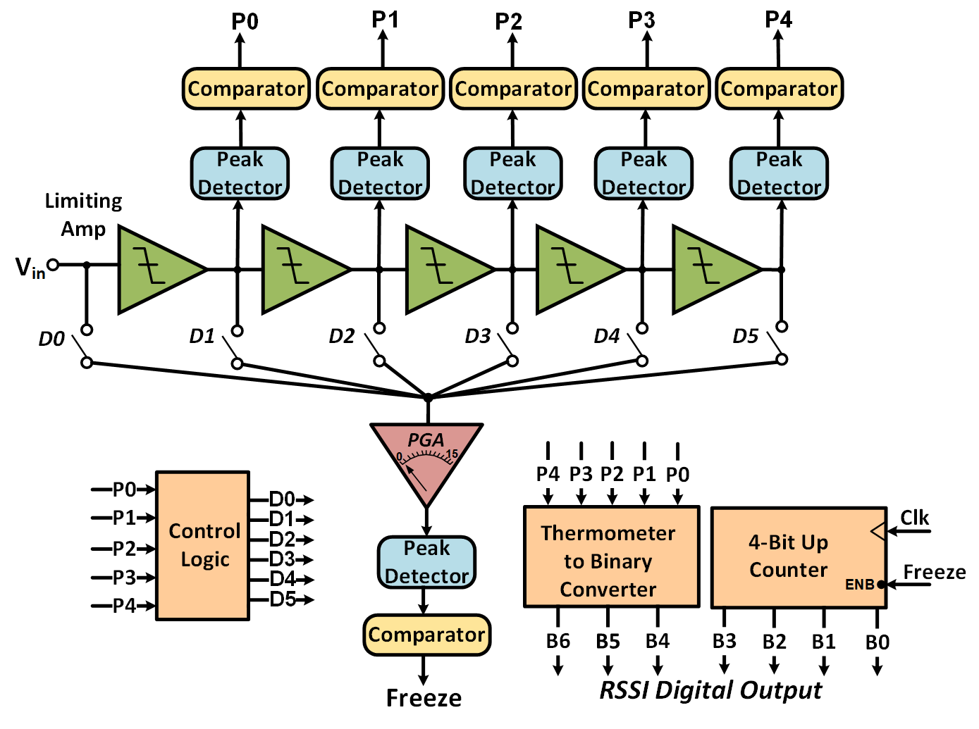
FAB & PROCESS SPECIFICATIONS
- Process Node:65 nm CMOS (TSMC 1P9M)
- Active area:0.39 mm²
- Status: Silicon-Proven / Production-Ready
ARCHITECTURAL HIGHLIGHTS
- Digital-intensive baseband RSSI with
- Wide dynamic range: 80 dB
- Detection accuracy: ±0.8 dB
- 7-bit digital RSSI output
- Programmable-gain amplifier (PGA) with 1-dB step size
Power Consumption Power Consumption < 0.8 mW – Operating Temp Range -40°C to +85°C (Industrial)
It support biologically inspired spiking and learning mechanisms while operating at very low supply voltages and power levels.
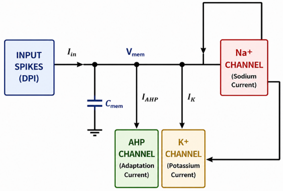
FAB & PROCESS SPECIFICATIONS
- Process Node:65 nm CMOS (TSMC 1P9M)
- Active area:0.188 mm²
- Status: Silicon-Proven / Production-Ready
ARCHITECTURAL HIGHLIGHTS
- Spiking Frequency: 30 Hz
- PBXCIP Neuron: 3.5 pJ/spike @ 0.5 V
- STDP Synapse: 1.2 pJ/learning event
- Neuron Area: 58 µm × 42 µm
Power Consumption
- Associative Memory:800 pW average power
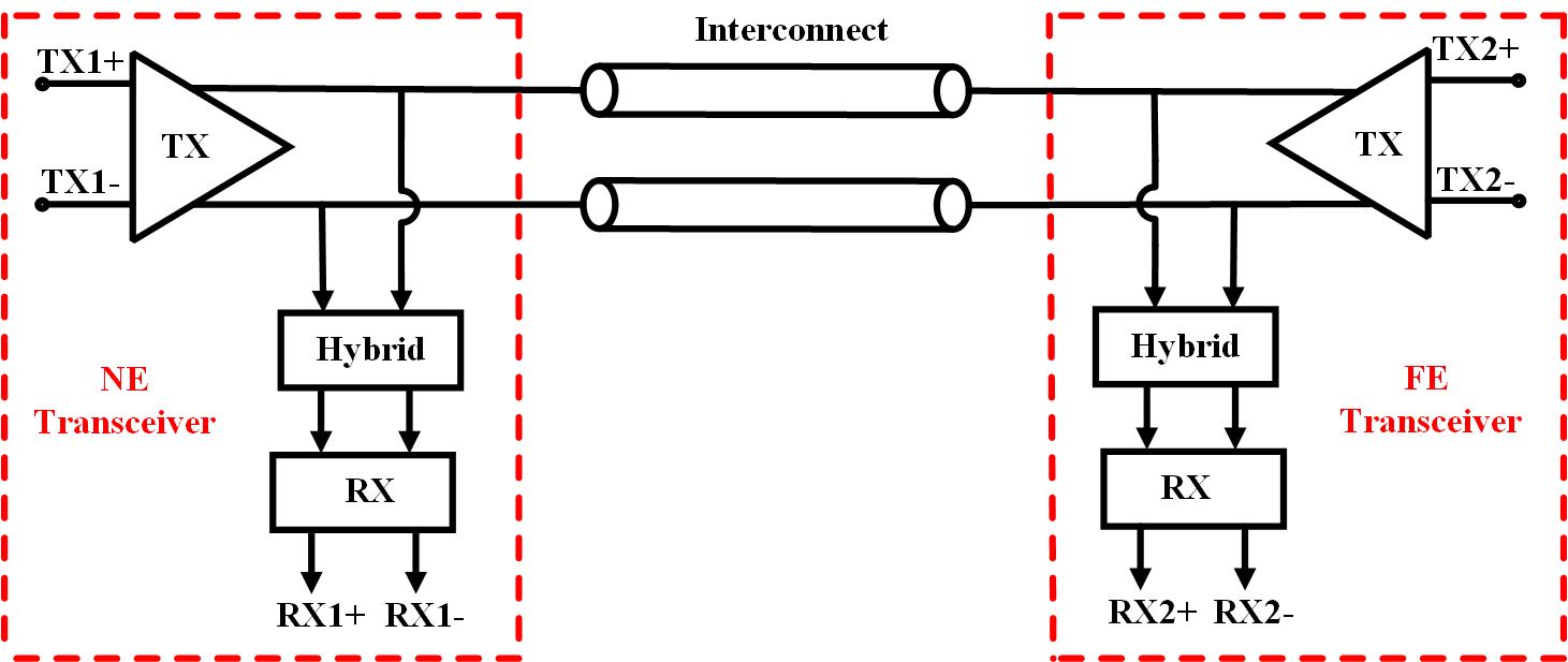
High-speed full-duplex chip-to-chip communication enables simultaneous bidirectional data transfer over a single interconnect. Consequently, a hybrid circuit is required to separate the received signal from the interconnect signal effectively.
FAB & PROCESS SPECIFICATIONS
- Process Node:65 nm CMOS (TSMC 1P9M)
- Active area:0.4 mm²
- Status: Silicon-Proven / Production-Ready
ARCHITECTURAL HIGHLIGHTS
- Data rate: 12 Gb/s full duplex
- Half-rate clock operation
- Strong-arm latch Hybrid power: 3.86 mW
- Bit Error Rate:10e-12
- Eye Opening:460mV
Power Consumption Power Consumption < 4 mW – Operating Temp Range -40°C to +85°C (Industrial)
High-speed full-duplex chip-to-chip communication enables simultaneous bidirectional data transfer over a single interconnect. Consequently, a hybrid circuit is required to separate the received signal from the interconnect signal effectively.
FAB & PROCESS SPECIFICATIONS
- Process Node:65 nm CMOS (TSMC 1P9M)
- Active area:0.4 mm²
- Status: Silicon-Proven / Production-Ready
ARCHITECTURAL HIGHLIGHTS
- Data rate: 12 Gb/s full duplex
- Half-rate clock operation
- Strong-arm latch Hybrid power: 3.86 mW
- Bit Error Rate:10e-12
- Eye Opening:460mV
Power Consumption Power Consumption < 4 mW – Operating Temp Range -40°C to +85°C (Industrial)